Home
SPI Bus Loopback Visualization on the STM32 Microcontroller
I’ve been gradually working through Geoffrey Brown’s Discovering the STM32 Microcontroller: it is awesome. I would bet money that there is not another resource out there as well put together as this one when it comes to introductory applicative microcontroller development. The complexity of both the hardware and software involved makes narrative instruction a challenge, but Geoffrey Brown nails it with his book and associated STM32 project template.
Time, as always, bedevils the desired longevity of instructive written word. The Saleae Logic application used throughout the book has been substantially updated, so a few parts require some translation and imagination. And since I ran into a few other hurdles while working through Chapter 6, I figured this would be a good opportunity to write them up for the next person that hits up the search engines for answers.
Chapter 6 is all about the SPI bus, and the first exercise involves looping the output (MOSI) back to the input (MISO) in order to easily visualize and verify everything with the Saleae Logic analyzer. The author, as usual, does an excellent job of stepping through the necessary code. He leaves SPI clock and pin configuration up to the reader, as is to be expected, since this information is covered generically in a previous chapter.
The first thing that stumped me though was the reference to function csInit() in main(). There’s no mention of it in the book, and I figured it must be additional clock/pin configuration code, but I turned to the Internet to be sure. My assumption turned out to be correct, as indicated by this ST forum post involving a discussion of csInit(), albeit for the STM32F429 line; with a little adaptation, I arrived at the following implementation suitable for the STM32VL:
void csInit(void) {
  RCC_APB2PeriphClockCmd(RCC_APB2Periph_GPIOC, ENABLE);

  GPIO_InitTypeDef GPIO_InitStruct;
  GPIO_InitStruct.GPIO_Pin = GPIO_Pin_3;
  GPIO_InitStruct.GPIO_Speed = GPIO_Speed_50MHz;
  GPIO_InitStruct.GPIO_Mode = GPIO_Mode_Out_PP;
  GPIO_Init(GPIOC, &GPIO_InitStruct);

  // Initialize chip select to high.
  GPIO_WriteBit(GPIOC, GPIO_Pin_3, 1);
}
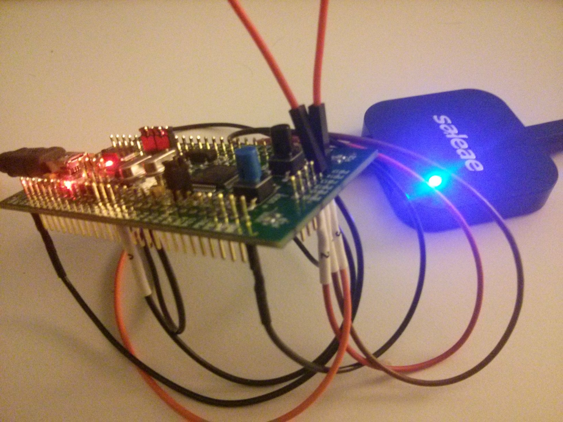
After adding that in, everything compiled, and I loaded the binary onto the STM32 (you can find my final working source code for this exercise here). I looped MOSI (PB15) into MISO (PB14), then attached the GND and channel wires for ports 0 through 3 of the Saleae Logic to the STM32, with the following channel wire to pin mapping:
- Channel 0: PC3 (SS line)
- Channel 1: PB14 (MISO line)
- Channel 2: PB13 (SCK line)
- Channel 3: PB15 (MOSI line)
I am using Logic 1.2.1 Beta, so the UI is markedly different from the screenshots in the book. In the application, I enabled data collection on channels 0 through 3, with channel 0 having a rising edge trigger. Unlike the application version that is referenced in the book, Logic 1.2.1 Beta’s data collection options do not involve selecting a sample number and frequency; the parameters are sample rate and duration instead. So, I set the sample rate to 1 MS/s (the lowest) with a duration of 5 seconds.
However, when I hit Start, then ran the program on the STM32, the data recorded by Logic only showed a single high-low-high transition on the enable (SS) line. Nothing on the SCK, MOSI, and MISO lines. I went about figuring out what clock-related configuration I had missed, and it turned out that I had enabled the clock for the SPI2 peripheral, but had forgotten to enable the appropriate clock for GPIOB, which uses a separate peripheral clock (see this thread). I modified the spiInit routine to include the following initializion lines:
RCC_APB1PeriphClockCmd(RCC_APB1Periph_SPI2, ENABLE);
RCC_APB2PeriphClockCmd(RCC_APB2Periph_GPIOB, ENABLE);
I then re-ran the program on the STM32 while re-capturing data in Logic, which yielded the following recording:
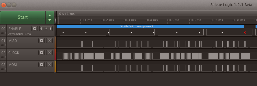
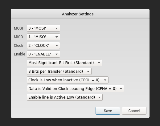
As can be seen in the screenshot, the clock signal is now coming through, and the MISO and MOSI lines show data on them as well. But that red “x” on the right hand side indicates a framing error, and Logic should be showing values for each byte clocked through on MOSI and MISO; instead, it’s showing 0x04 across multiple read/write sequences. The solution took me awhile to realize but it turned out to be simple: I was erroneously using the Async Serial analyzer left over from Chapter 5’s USART exercises, when I should have been using the SPI analyzer instead. On the right hand sidebar in Logic, I removed the Async Serial analyzer, then clicked the “+” button to add the SPI analyzer:
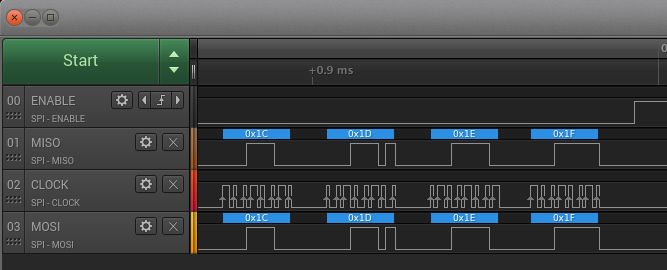
Take a few extra seconds to carefully check the channel mappings in that dialog; I rushed through it the first time and didn’t realize MOSI and ENABLE were switched, leading Logic to annotate the simple transitions on the ENABLE line rather than the actual data on MOSI. All of the other defaults are correct for this particular case. Once you’ve verified the channel mappings, click “Save”; Logic should now be displaying decoded values for the MISO and MOSI lines. Now we can see that the last of the eight read/write sequences of four 8-bit values is correctly decoded by Logic as:
And later on, the last of the eight read/write sequences of four 16-bit values is correctly decoded by Logic as:


